 "Together we can significantly impact the growth and development of technology within the state of New York with the added potential to establish the New York State Nanotechnology Network (NNN) as a partnership model committed to the advancement of nanotechnology across disciplines in the United States".
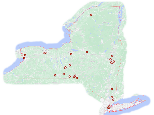
The below New York State institutions are partnering and expanding technology skills and capabilities while providing synergies that are strengthening technology and the workforce in New York State.
Through training, research and testing, CEMA prepares professionals to become successful within a global society. CEMA leverages this:
- To be a Center of Excellence in understanding and supporting the needs of the electronics packaging industry.
- To provide relevant services to our industry partners, engaged in semiconductor chip packaging, printed circuit board assemblies and electronics/optoelectronics systems.
CNI Shared Laboratories provide access to cutting-edge equipment and services for student and faculty researchers at Columbia University, external academic institutions, as well as researchers from government, entrepreneurial ventures, and industrial companies. The shared facilities include a wide range of micro and nanofabrication processing, characterization, and imaging instruments. The CNI Nano Fabrication Clean Room offers access to a comprehensive set of tools for micro-/nano-fabrication for applications such as nano-electronic/photonic devices, micro and nano-electromechanical systems (MEMS/NEMS), flexible electronics, nano-bio interfaces, and more. The Materials Characterization Laboratory and the Electron Microscopy Laboratory provide access to state-of-the-art instruments for chemical and structural characterization of materials at the micro- and nanoscale.
CNI's PhD level staff work as partners with CNI users, providing consultation and training as well as maintaining the facilities 24/7. In a normal year, it supports 400 users. Research centers funded by the NSF, DOE, DOD, and outside foundations in the areas of nanotechnology, photonics, and quantum among other fields, rely on these facilities. Terms, conditions, and contacts for external users are provided on the CNI Labs web-site.
CNF holds a proud history of experience as a national and international user facility. For 45 years, CNF has proven its commitment to the advancement of science and technology through continued support of academic, industrial, and government research communities. CNF serves as an open resource to scientists and engineers extending across a broad range of nanotechnology areas. CNF focuses primarily on providing complex integration capabilities supporting individual user micro - nanofabrication needs.
CNF prides itself on its seasoned staff who work diligently to serve and address the needs of the user community. The CNF technical staff consists of facility and equipment technicians, process, and tool engineers (B.S./M.S.), and Research Associates (Ph.D.). Their extensive expertise enables high equipment uptime, thorough training, and provision of valuable technical advice. CNF offers an affordable hands-on 24/7 facility with over 180 outstanding tools and capabilities benefiting both research and prototyping initiatives.
CNF maintains a full complement of processing and characterization equipment and has the most advanced e-beam lithography facilities in the NNCI network including, but not limited to g-line, i-line and DUV stepper lithography; nanoimprint; contact aligners; 17 plasma etchers; 20 furnace tubes; graphene and carbon nanotube deposition; CMP; 3D printing; physical and chemical vapor deposition; plasma-enhanced CVD deposition; atomic layer deposition; molecular vapor deposition; in-house mask makers; rapid thermal processing; electron microscopy; atomic force microscopy; wafer bonding; wire bonding; packaging; electrical testing; and an extensive suite of and modeling software.
Odyssey Semiconductor Technologies Inc. is a micro-cap publicly traded company focusing on product development using internal R&D of semiconductor materials, processes, and devices. Founded by Dr. Rick Brown and Dr. James R. Shealy, the company is commercializing disruptive proprietary technology that would enable gallium nitride (GaN) to displace silicon carbide (SiC) as the dominant high voltage power switching semiconductor material of choice
The material properties of GaN make it the superior option for high voltage power switching applications. Previously, GaN processing technology has not been able to produce a viable high voltage switching transistor operating above 1,000 V. Contemporary devices are largely horizontal conduction devices based on radio frequency (RF) designs modified to operate at high voltage. These designs are not scalable beyond 1,000 V, which limits their use to low voltage, consumer electronics. Odyssey Semiconductor’s unique GaN processing technology allows for the realization of vertical conduction GaN devices, which extends voltages beyond 1,000 V. This dramatic improvement in performance allows GaN power switching devices to extend well beyond the consumer electronics space into more demanding areas such as electric vehicles, industrial motor control, and energy grids. While Odyssey Semiconductor’s proprietary vertical conduction power switching transistors can operate below 1,000 V, this market is well served by the GaN-on-Si HEMT devices currently available. Odyssey Semiconductor is targeting a much higher power device market than is currently being served by SiC.
Odyssey Semiconductor operates a 10,000 sq. ft semiconductor design, fabrication, and testing center in Ithaca, NY. The fabrication facility is vertically integrated for the development of all aspects of GaN power switching devices.
Odyssey Semiconductor also offers a semiconductor device development and foundry service, filling the gap between university labs and larger-scale wafer foundries. Odyssey Semiconductor specializes in rapid small-batch prototype and pre-production wafer runs utilizing a variety of materials. Wafer starts available with minimal investment cost.
For 20 years Phoebus has performed advanced research and development in metamaterial structures, optical components, and optoelectronics for clients. We specialize in developing and fabricating hyperspectral and multi-spectral sensors in the short, mid, and long-wave infrared spectral regions with customer-specified optical performance, such as low angle of incidence dependence and narrow bandwidth filters. We design optical components for a variety of imaging, sensing, and biosensing applications.
Phoebus services: Innovation, Design, Modeling, Fabrication, and Optical Testing.
Phoebus PhD level scientists can perform for customers modeling and simulation tasks, including the modeling of electrically large devices in the frequency and time domain, eigenmode analysis, asymptotic ray tracing, integral equation method, full-wave 3D analysis. Our high-performance cluster can solve ~1.5 billion mesh cells in the time domain. Additionally, Phoebus has proprietary software that provides an unprecedented level of detail of electromagnetic modes and rigorous coupled plane wave analysis. Phoebus works closely with customers to innovate; design and model structures of interest; and fabricate and test prototypes to demonstrate technical merit and economic feasibility. Phoebus scientists have experience working with Si, III-V, II-VI semiconductor materials, oxides, nitrides, and other materials.
The SUNY Polytechnic Institute College of Nanoscale Science and Engineering’s Innovation Lab is a collection of cleanrooms and laboratories that provide faculty, external partners and users with strategic support through technology acceleration, proof of concept, pilot prototyping, and test-bed integration for next generation nanotechnology research activities. These facilities are also home to multiple centers including the NY State Center for Advanced Technology in Nanomaterials and Nanoelectronics (CATN2) and NY State Center of Excellence in Nanoelectronics and Nanotechnology (CENN). Projects performed in these labs tend to focus on traditional and emerging applications in the areas of nanoelectronics, microsystems, nanobioscience, and clean energy.
The labs contain a full complement of leading edge tools to convert ideas into reality with processing capabilities that include: thin film deposition, wet etch, deep reactive ion etch, dry etch, wafer bonding, polymer processing, wafer patterning, and handling of multiple wafer sizes up to and including 200mm of varying materials including silicon, glass, SiC and ceramic substrates. Projects performed within the Innovation Lab have access to SUNY Poly faculty subject matter experts and the added capabilities of the entire Albany Nanotech Complex and its world-class 300mm wafer scale fabrication facilities for rapid proof of concept and manufacturing scale up.
SUNY Polytechnic Institute’s Nanoscale Metrology and Imaging Center is available to researchers and technology development partners that are hosted on campus. The center also provides its characterization expertise to third parties with the objective to assist local and regional colleges, universities and companies in their research and development efforts. In addition to these assets, SUNY Polytechnic Institute houses advanced electronic measurement and characterization capabilities, from small sample to full 300mm wafer. These capabilities are further enhanced with a continuum of high voltage (HV) testing equipment (up to at least 20 kV) for on-wafer characterization, high performance characterization, and HV and high temperature reliability and ruggedness testing.
As a result of these world-class resources and capabilities, as well as faculty expertise, SUNY Poly provides a range of workforce training opportunities (undergraduate, graduate, and professional-level) in the critical innovation-centered fields, from nanoscale science and nanoscale engineering, along with nanobioscience at its Albany campus, to engineering and advanced technology at its Utica campus.